Microsoft Sculpt Wired Conversion Mod
I made a control board for the Microsoft Sculpt wireless keyboard that converts it to wired USB, and now my favorite keyboard is even better.
The QMK config is available at @chadaustin/qmk_firmware (keyboards/handwired/sculpt/), and the PCB design files at @chadaustin/wired-sculpt-pcb.
I’m planning on making at least one more, so if you’d like one, maybe I can help.
It’s a huge improvement. Latency is reduced by about 13 milliseconds, and with full control over the microcontroller’s firmware, you can customize keymaps and layers, and actually use the keyboard’s built-in LEDs.
Why?
Feel free to stop reading here — I am going to tell the sequence of events that led to this project. Besides some exposure to basic voltage and resistance circuits in college, I have very little electronics background. But, in a short time, I went from only barely knowing what a capacitor was to having a working PCB manufactured and assembled, and maybe this will inspire someone else to give it a try.
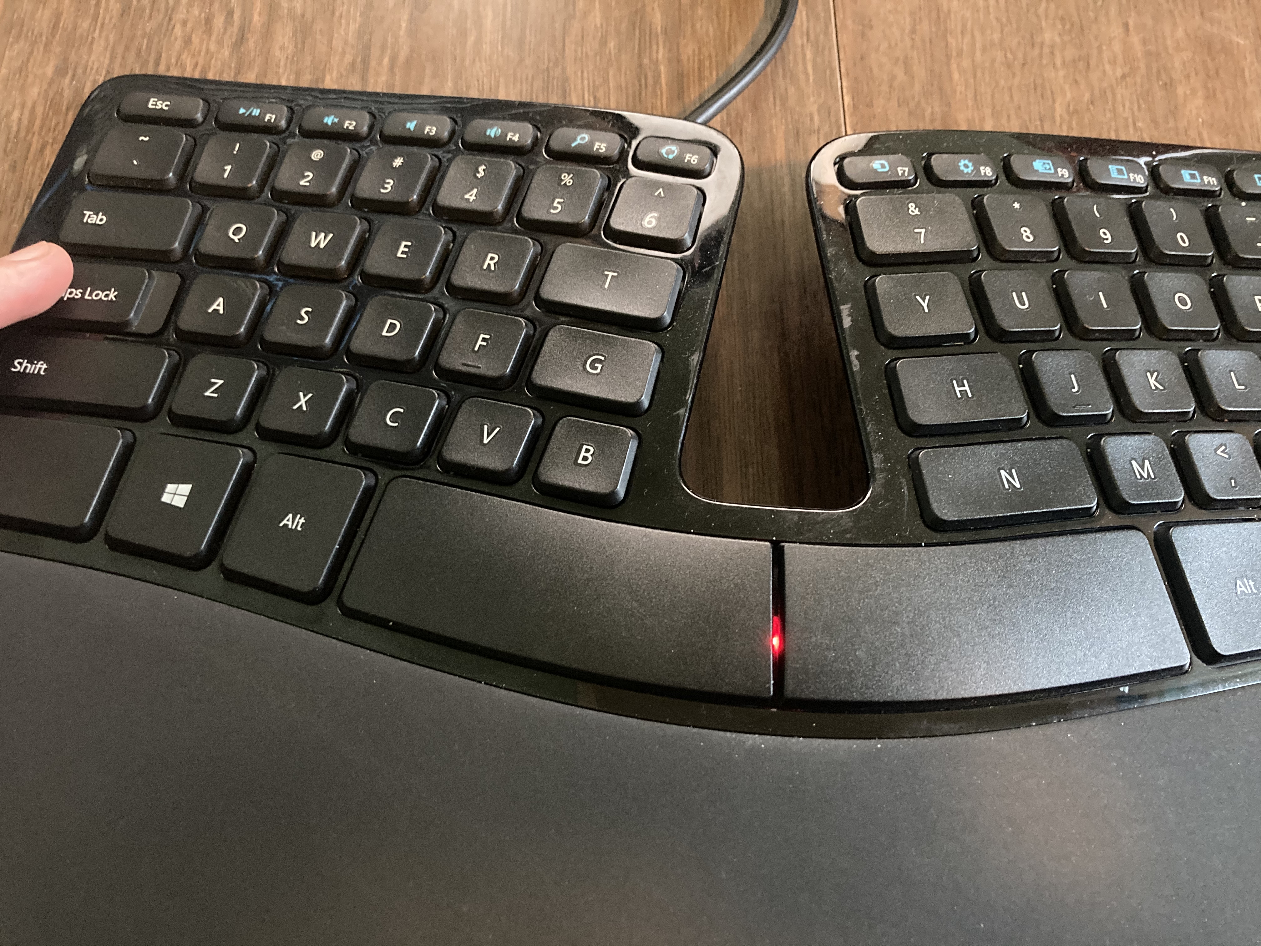
Since developing RSI in college, I’ve exclusively used Microsoft’s ergonomic keyboards. And when I first tried the Sculpt, I instantly knew it was the best yet. The soft actuation, short key travel, and rigid frame are perfect for my hands. And because the number pad is a separate device, the distance to my mouse is shortened.
My brother went out and bought one too. Not much later, he gave it to me, saying the latency was inconsistent and high, and it was unacceptable for gaming. I thought he was being uniquely sensitive, since I had no problem in either Linux, Windows 7, or macOS. But then I updated to Windows 10 and saw exactly what he meant.
It was like the keyboard would go to sleep if a key wasn’t pressed for a few seconds, and the first keypress after a wake would be delayed or, worse, dropped.
And heaven forbid I use my USB 3 hub, whose EMI would disrupt the 2.4 GHz signal, and every other keypress would be unreliable. I’d gone as far as mounting the wireless transceiver directly under my keyboard, on the underside of my desk, and keys were still dropped.
So, best keyboard ever. But wireless sucks. (But mostly in Windows 10? No idea about that.)
Over the Hump
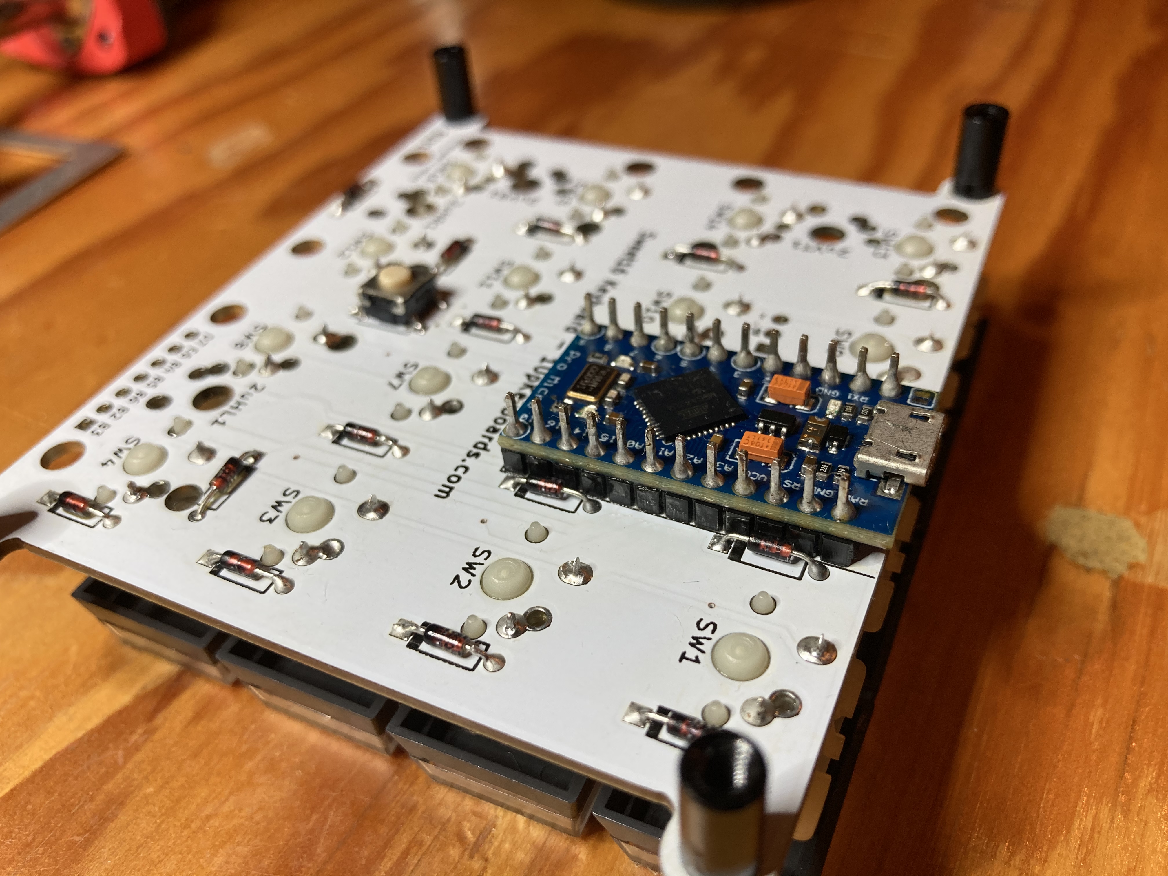
What started this whole thing is that the EdenFS team was a bunch of keyboard enthusiasts. During the pandemic, as we’re all at home burning out and missing each other, we were trying to think of some virtual team offsites. Wez offered to walk everyone through building a Sweet 16 Macro Pad.
So, okay, a keyboard is a matrix, with some diodes used to disambiguate the signalling, and a microcontroller that rapidly polls the matrix and reports events over USB…
So maybe I could fix the Sculpt! I bought a transceiver-less Sculpt off eBay for cheap and popped it open (thanks Emmanuel Contreras!), thinking maybe its controller could be flashed with new firmware that speaks USB. The Sculpt uses a Nordic Semiconductor nRF24LE1, but I was nowhere near capable of making use of that information at the time, though it did point me to Samy Kamkar’s horrifying guide on surreptitiously sniffing keystrokes from nearby (older) Microsoft wireless keyboards.
I almost gave up here, but Per Vognsen suggested I scan the matrix myself and it turns out Michael Fincham had already mapped out the matrix and soldered a Teensy 2.0++ board onto the Sculpt’s test pads, showing this was doable!
So I ordered my own microcontroller to try the same thing.
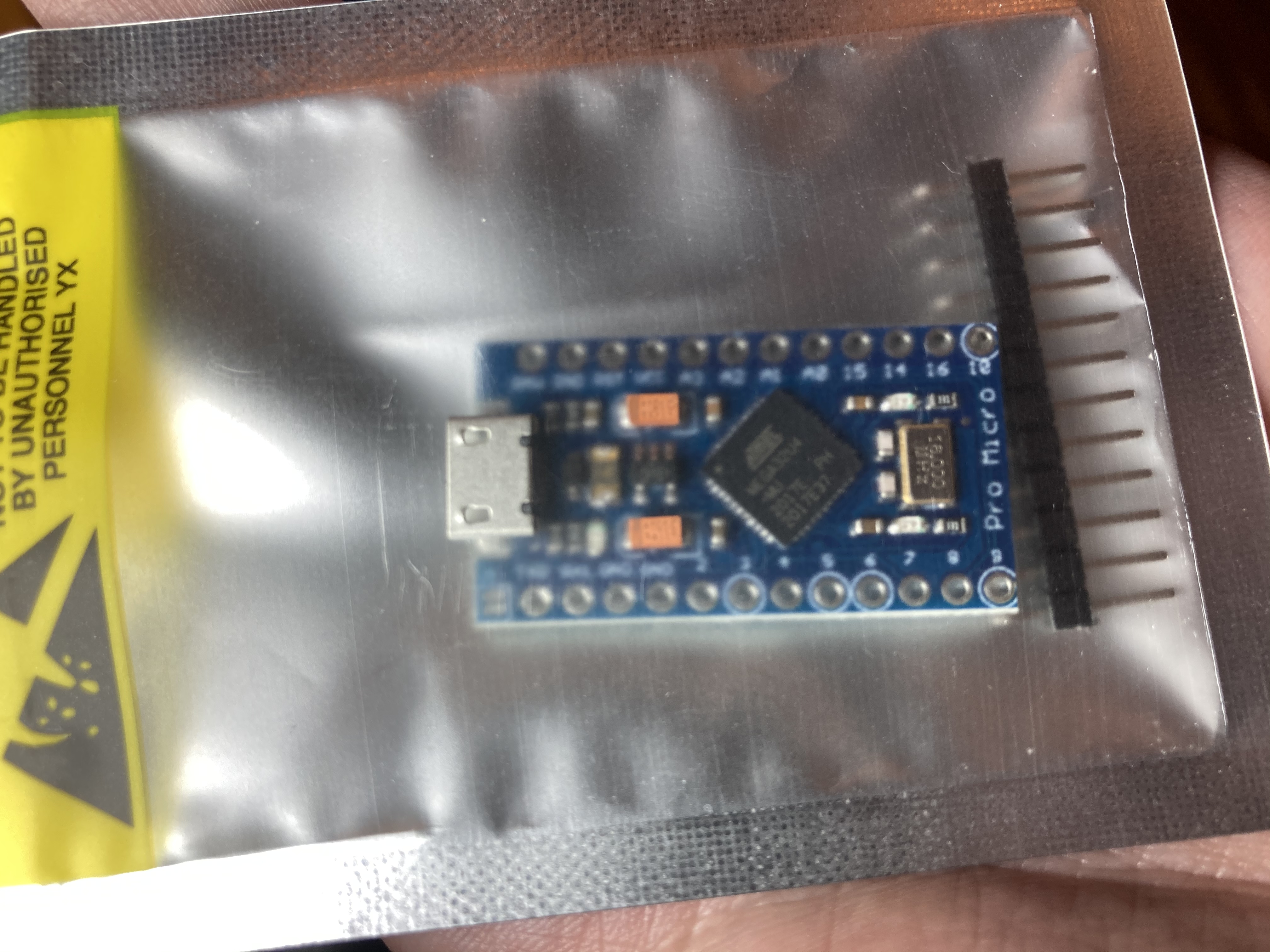
First, I bought an Arduino Pro Micro, like the Sweet 16 uses. Oh hey, 18 GPIO pins isn’t enough to drive the Sculpt’s 26-pin matrix. I looked at using an I2C GPIO expander, but it felt like taking on too much.
More pins? QMK’s Proton C has more pins! So I carefully soldered onto the test pads as Michael had shown was possible… and it worked!
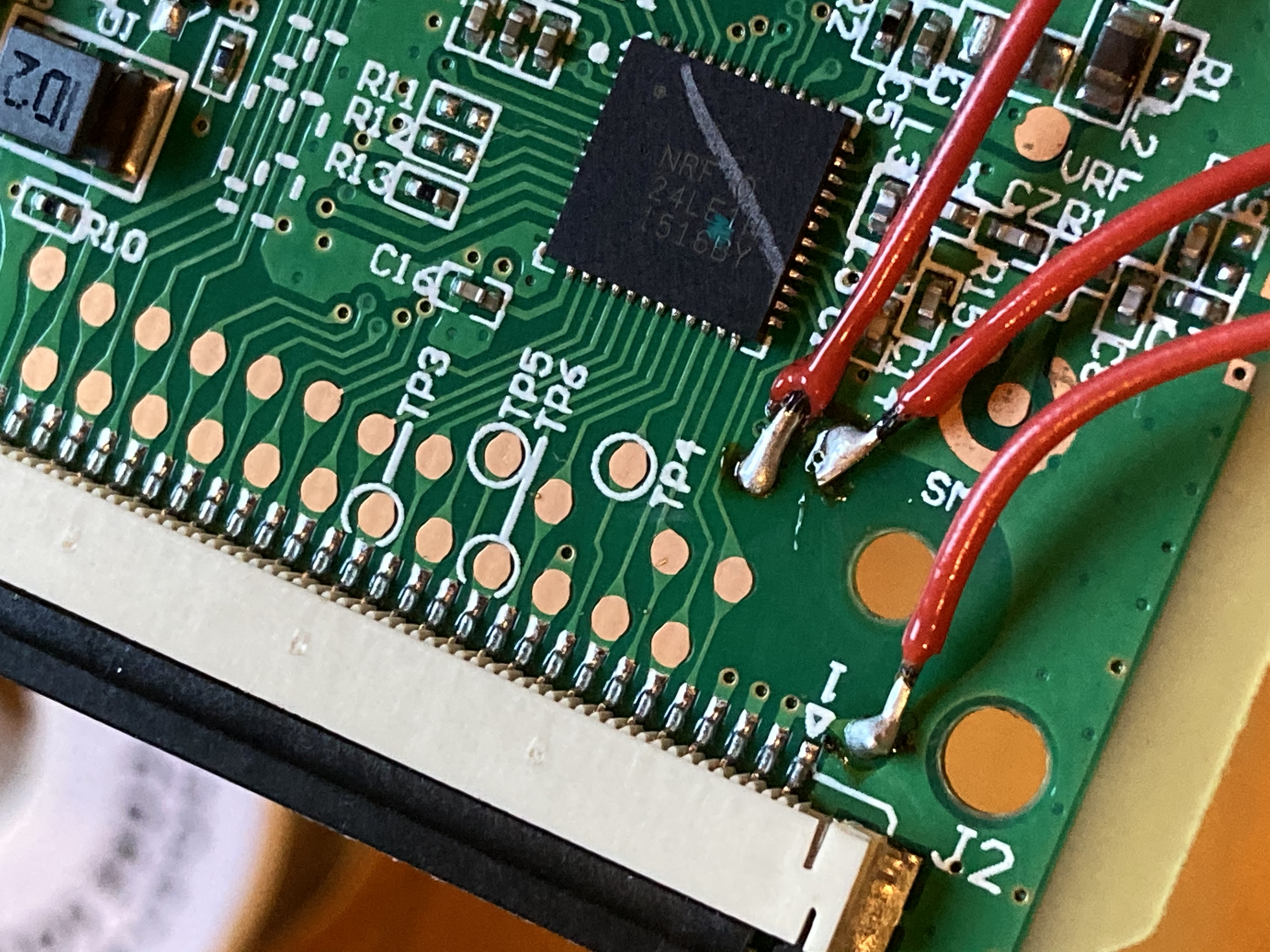
Getting those wires to stick to the pads without shorting was tricky. (I hadn’t yet discovered how magical flux is.)
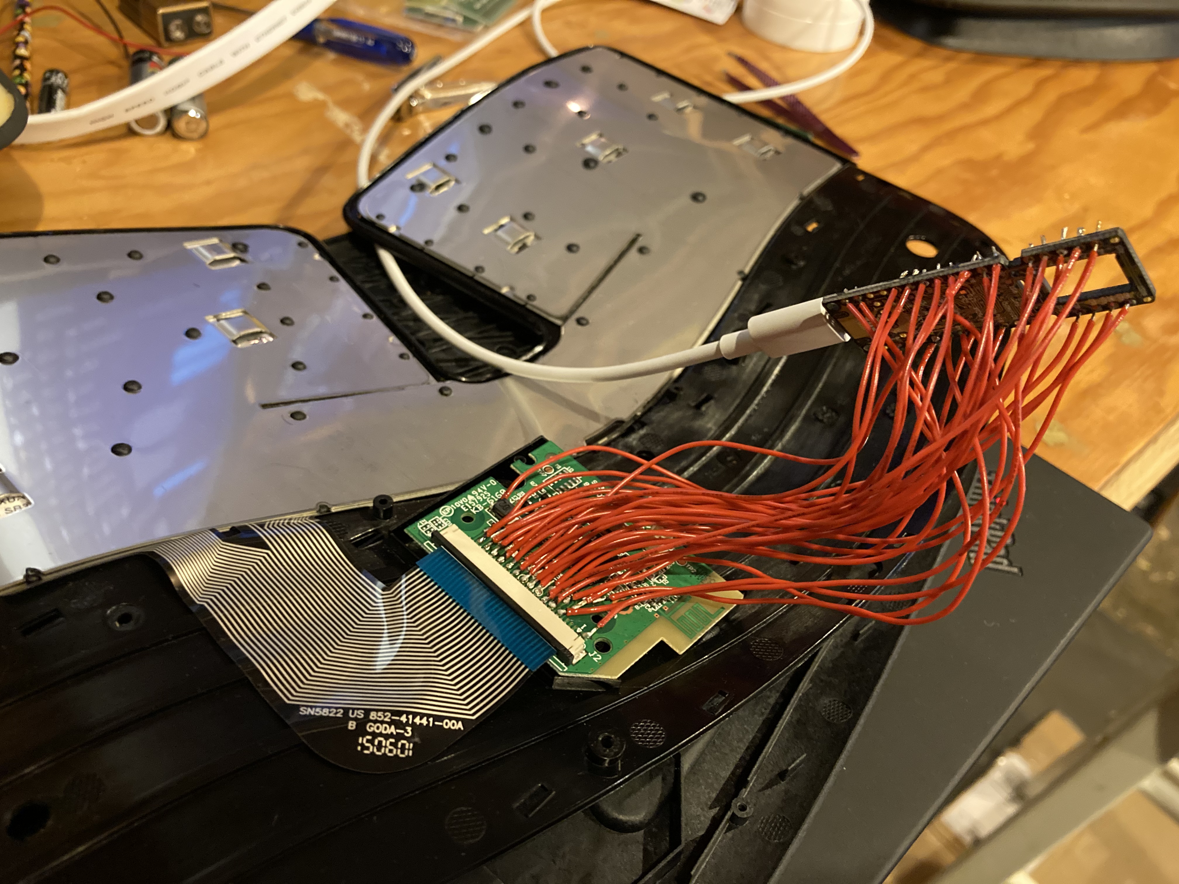
The keyboard worked, but I couldn’t fit the board, its wires, and the new microcontroller into the case, and I wasn’t really happy leaving it in this state, even if I could pack it in somehow.
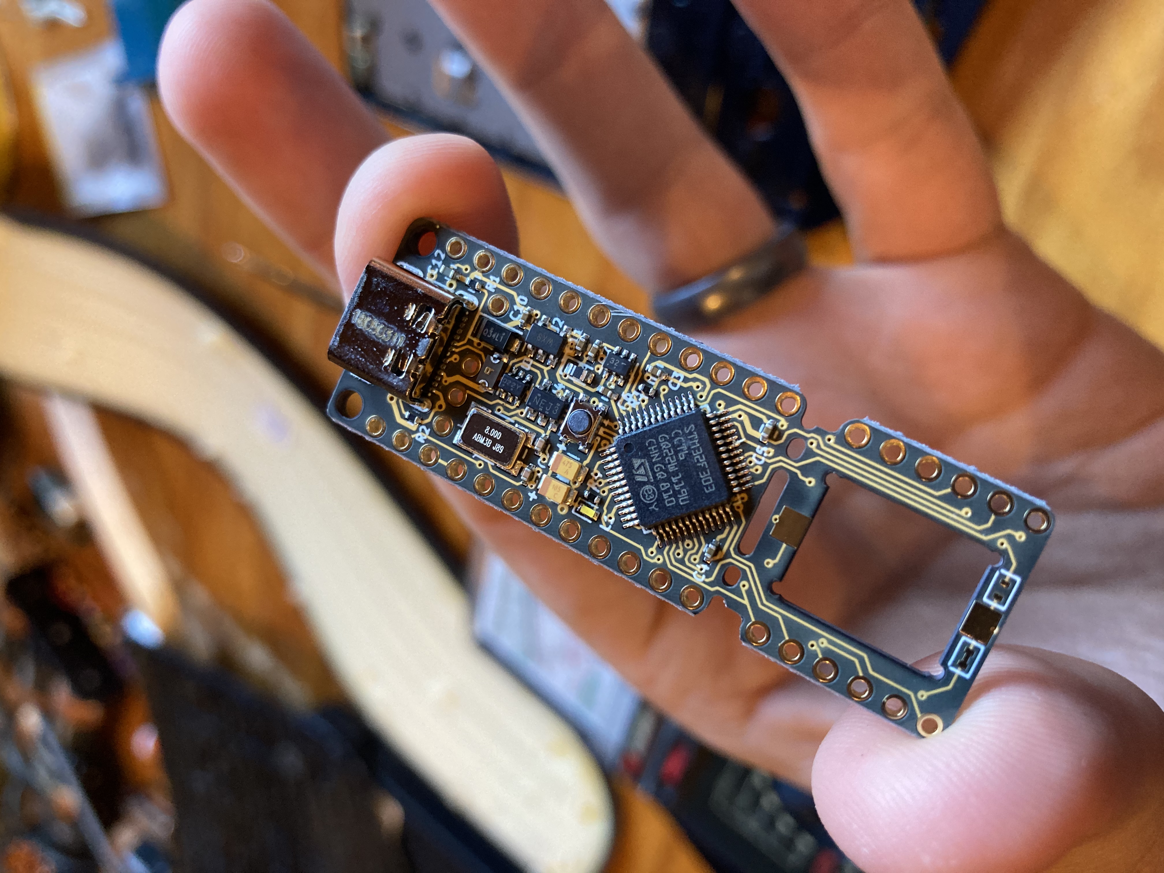
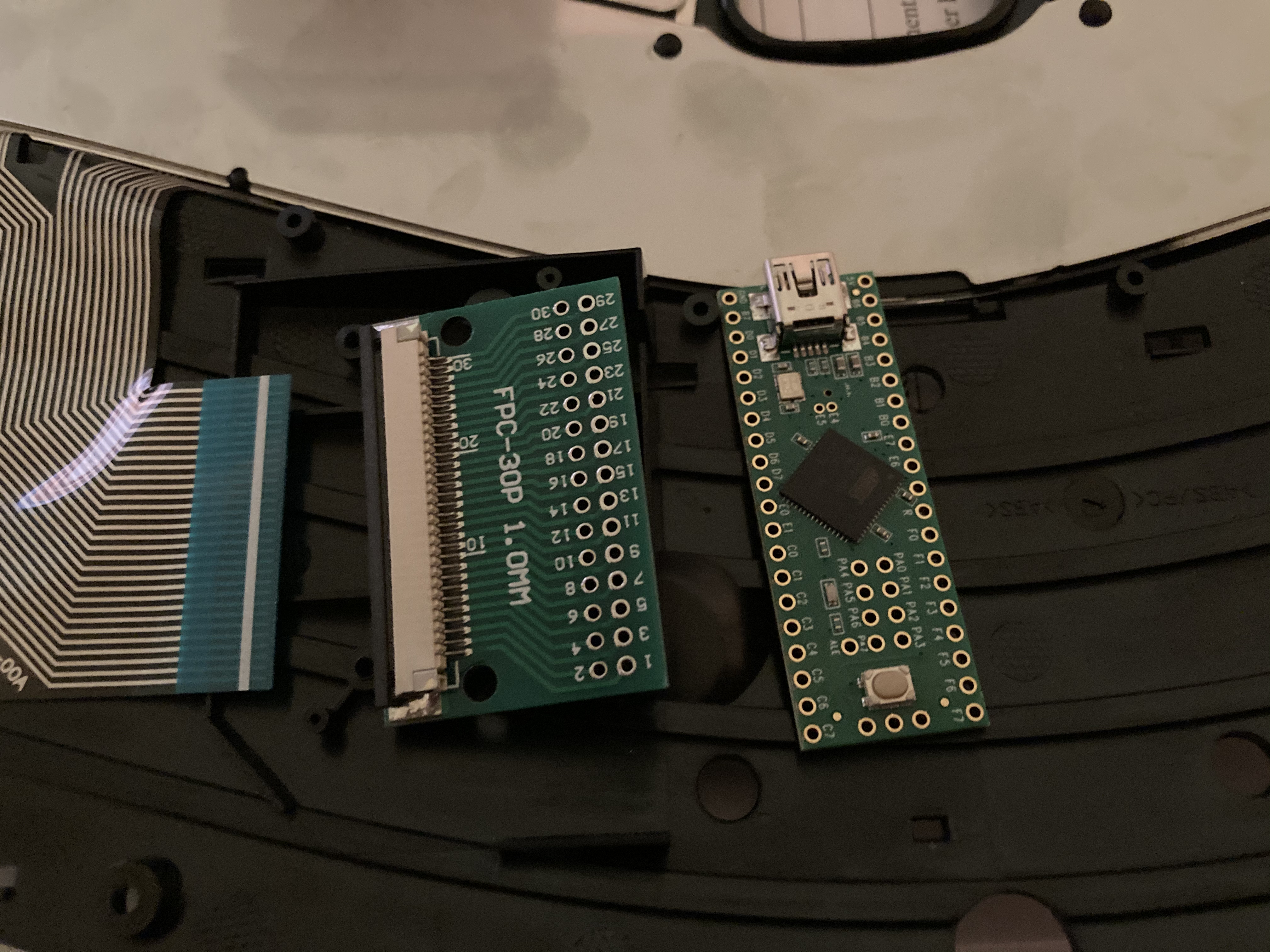
I thought, all I really need is the ribbon cable connector, so I ordered a 30 pin, 1.0 mm pitch ribbon breakout and the pricier (but tons of pins!) Teensy 2.0++. Looking back, it’s cute that I was trying to save $10 on the microcontroller… You just have to get used to spending money on whatever saves you time.
Well, it was almost as annoying to solder, and still didn’t fit. So much for saving money on microcontrollers.
I thought about giving up. Is it really that bad that my keys don’t always register in games? Can I just tolerate some flakiness and latency?
But Jon Watte offered to spend an entire day showing me how to use KiCad, design circuits, layout PCBs, select components on Digi-Key, scan datasheets for the important information, and how to work with a PCB manufacturing house. Of course you never turn down opportunities like that.
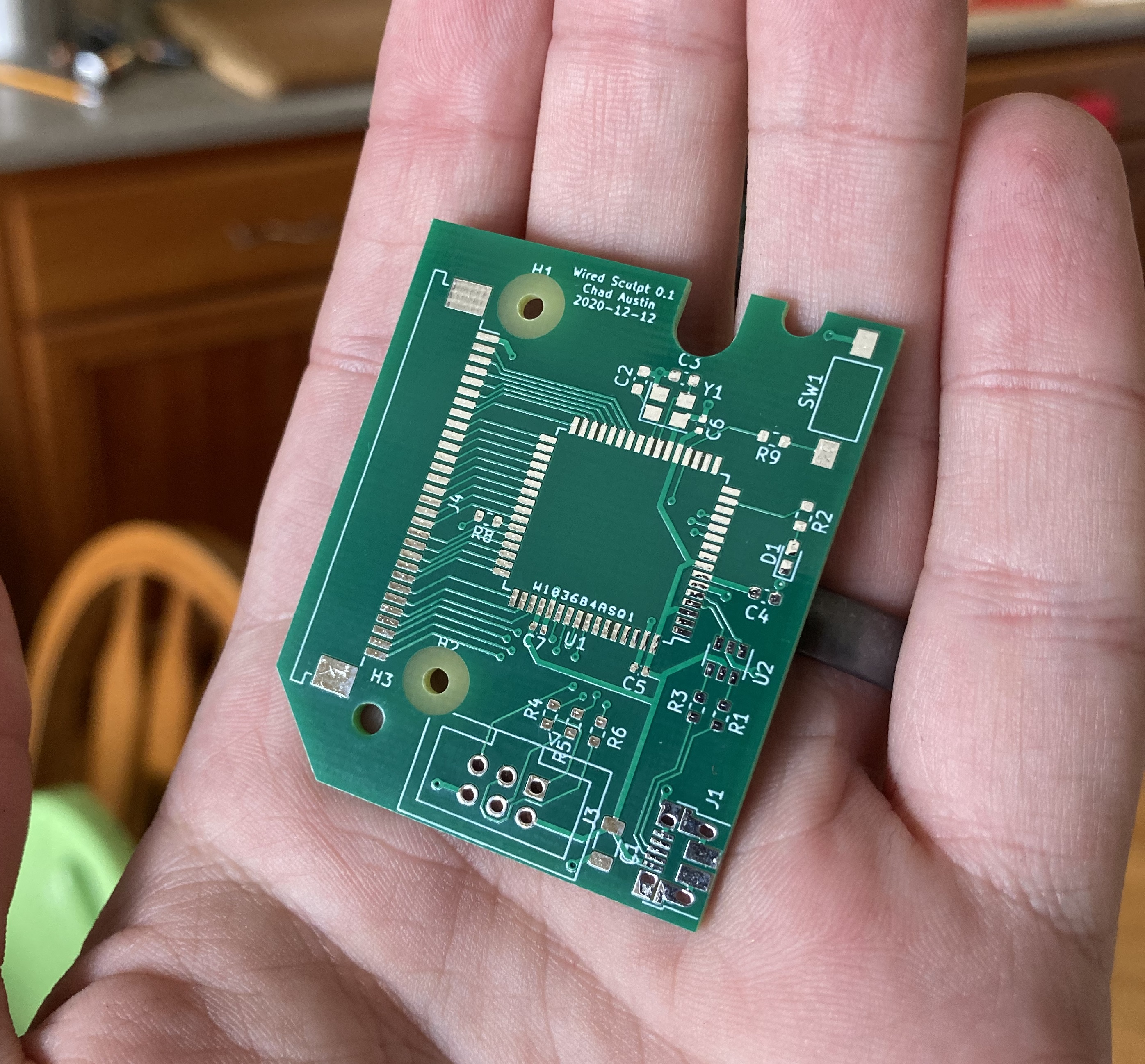
Designing the Final Board - Schematic
Assuming, like me, you’ve never done this, I’ll summarize the steps.
First you sketch out the circuit schematic.
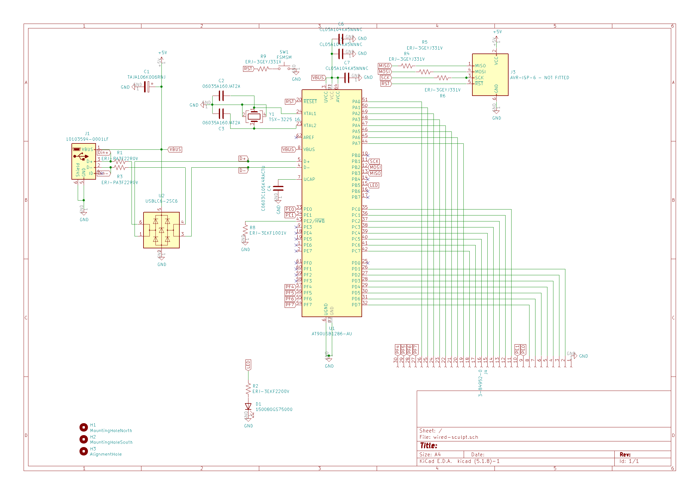
Jon showed me several tricks in KiCad, like global labels, and starting with some standard resistor and capacitor values, but it’s very important that you go through the datasheets, because details can matter a ton.
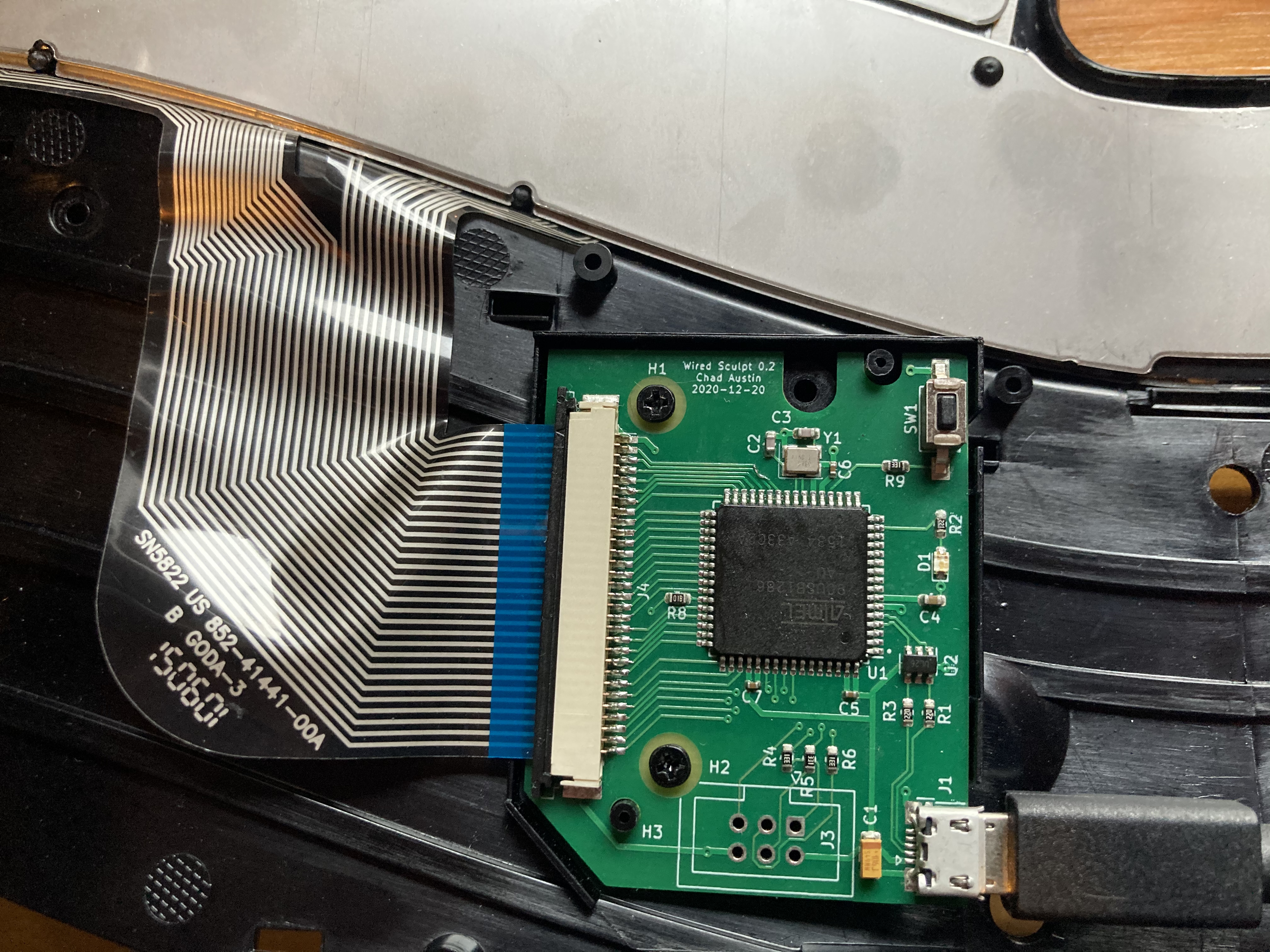
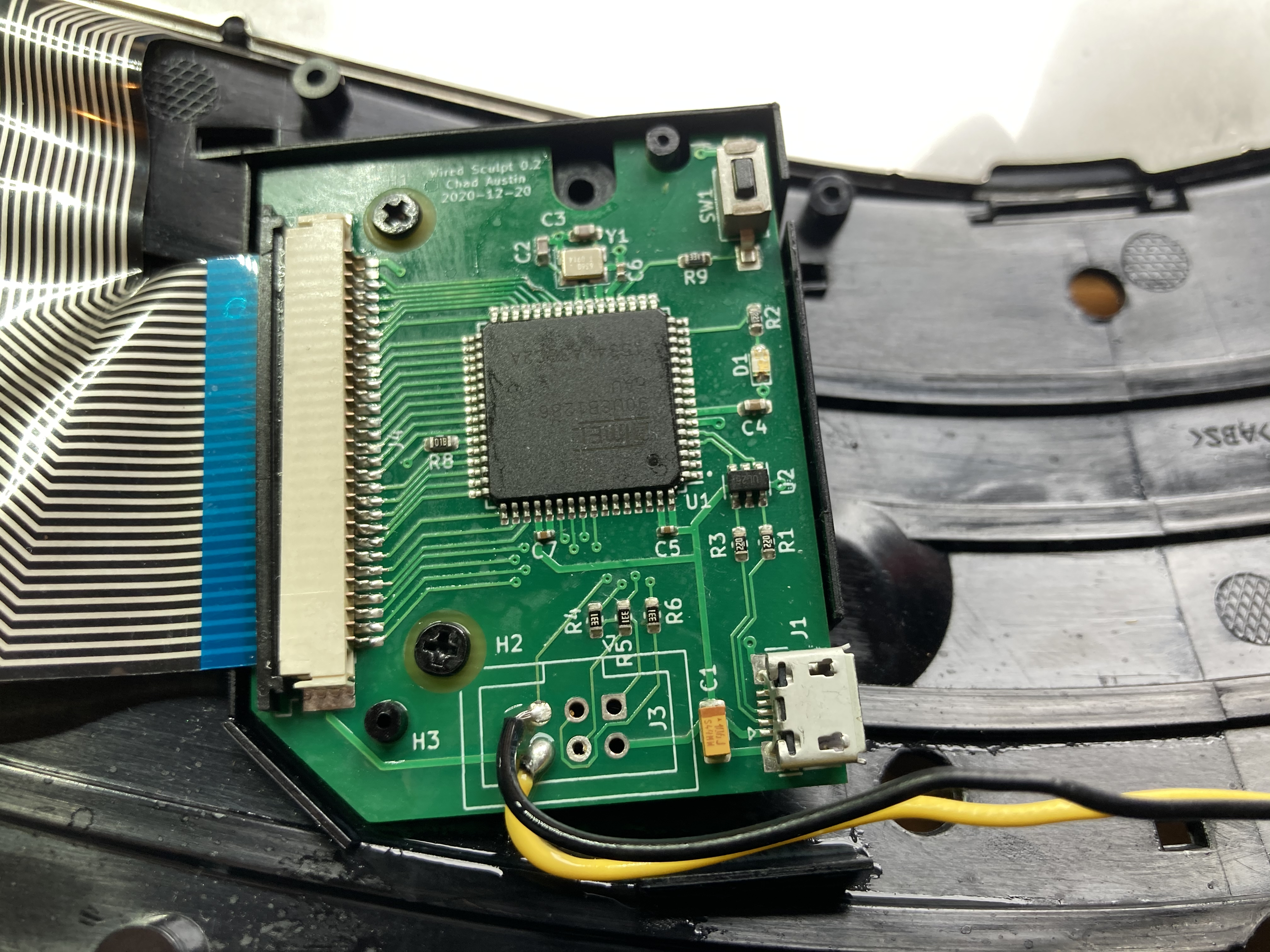
I knew I wanted the main processor to be the AT90USB1286 controller, and fortunately KiCad already had a symbol for it. Atmel has a comprehensive and accessible data sheet, which showed me I needed some 22 Ω resistors on the USB data lines, which of the ISP programmer lines needed resistors (and appropriate values), and that I needed to either pull HWB low, or provide a physical switch that pulls it low, in order to allow rebooting the device into USB firmware update mode.
There are a bunch of things that are implicitly known to electrical engineers but that were new to me. You want:
- a ground plane under the data lines and most of the microcontroller if possible.
- an electrolytic or tantalum bypass capacitor on the main 5V power from USB.
- ceramic filter capacitors on each power pin.
- appropriate values for the resonance capacitors on your crystal.
- electrostatic discharge protection! Turns out transients are common and it’s easy to fry a chip just by plugging it in.
And then when you get into concerns like EMI and high-frequency signal integrity, the rabbit hole goes deep.
I kept having to tell myself “it’s just a keyboard”, but it also helped that there are a great number of high-quality resources on these topics just a click away. I spent lots of time on EEVBlog.
Before finishing the circuit design, Jon had me do a couple smart things. In case the factory-supplied USB bootloader didn’t work out, he suggested I add the footprint (but not a connector!) for an ISP programmer and a debug LED to prove code would work at all.
Designing the Final Board - Physical Layout
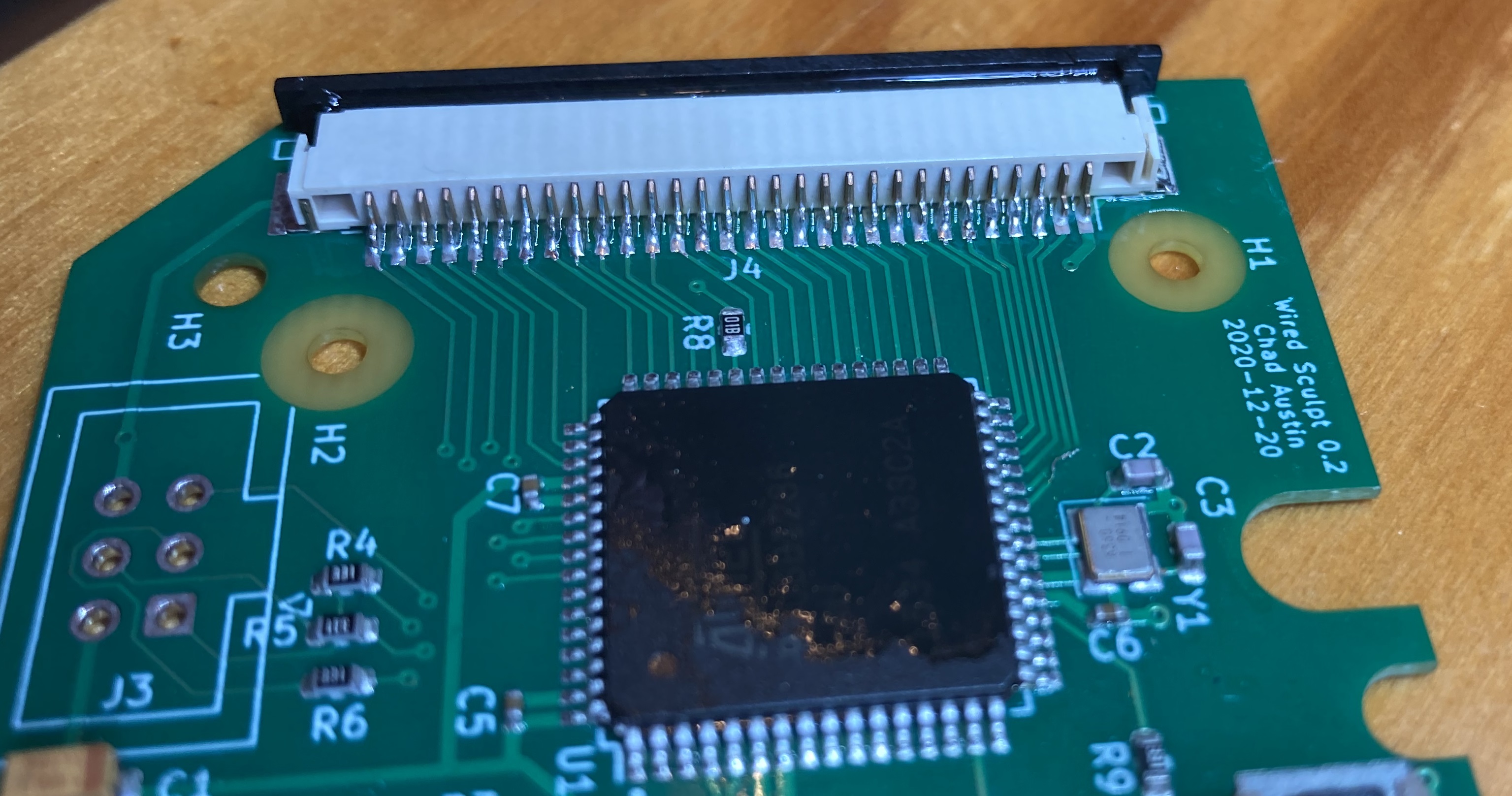
After arranging the schematic and ensuring it passed the electrical rules check, it was time to pick specific components. That is, the reference to a 220 Ω resistor is replaced with the Panasonic ERJ-3EKF2200V, 0603 surface mount.
There are a couple things to keep in mind. For common components, like resistors and ceramic capacitors, there is a huge amount of choice. For example, I see over 1400 surface-mount 220 Ω resistors on digikey. I tried to just stick with one high-quality brand like Panasonic or Samsung for all of that stuff.
The important thing is the physical form factor, which determines the footprint on the board. Once you pick a part, it has a size, and you need to tell KiCad which physical footprint should be assigned to that component. I used 0603 resistors, so I assigned each resistor in the schematic the “Resistor_SMD:R_0603_1608Metric” footprint.
Same for everything else. Jon showed me how to draw my own footprints, but to avoid complexity, I was able to find appropriate footprints in KiCad’s standard libraries for every component I needed.
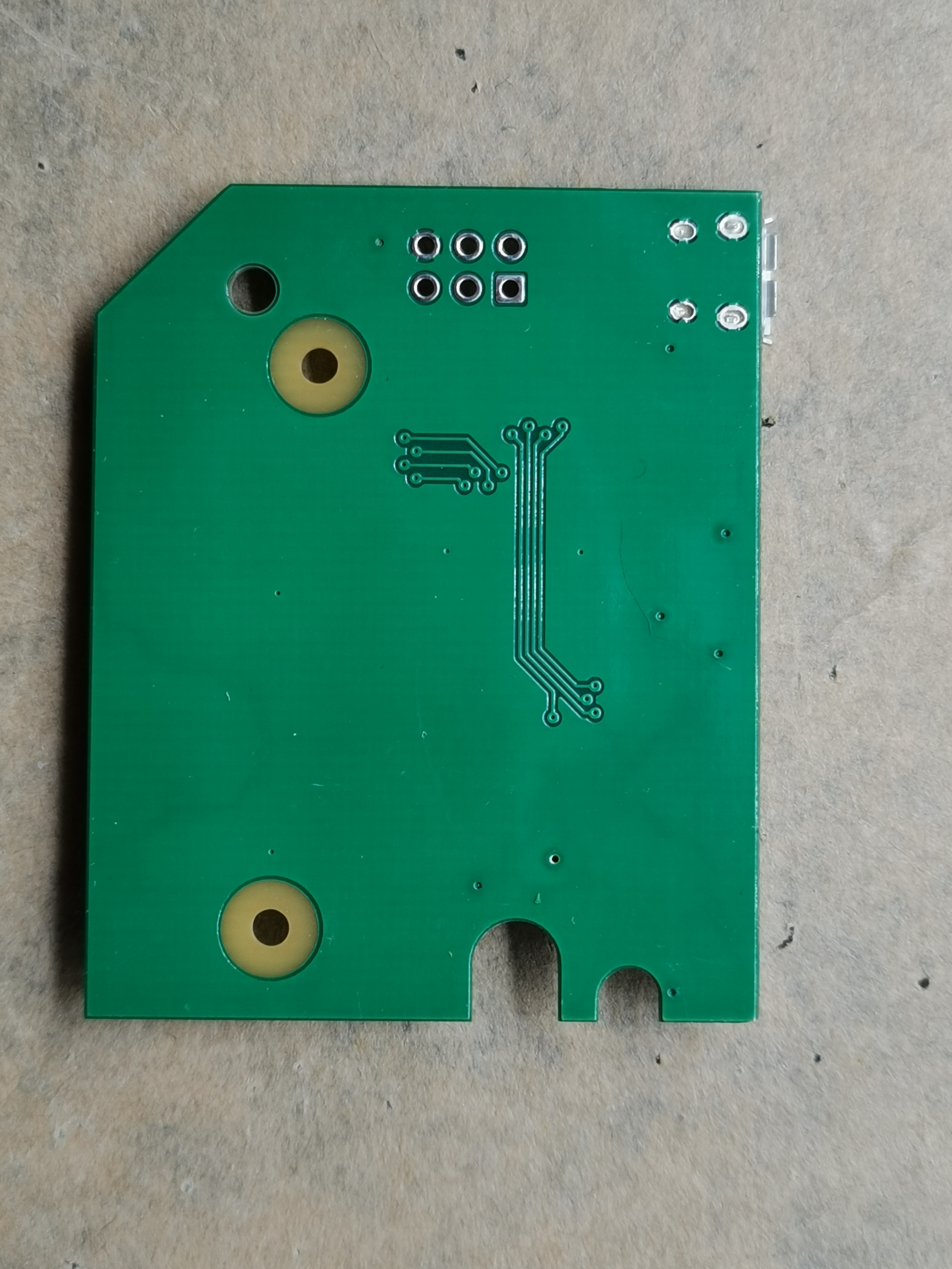
When you import the schematic into Pcbnew, it’s time to figure out where things go. Where are the edges of the board? Make careful measurements here. Where do the mounting holes go? Where do you want the microcontroller? Where do you want the USB port?
Also, you have to pick through-hole sizes and trace widths. Jon had me use .250 mm for the narrow traces and .500 mm for the wider ones, presumably from experience. I used the narrow traces for signalling and wide traces for power, though I’ve since heard it’s a good idea to use narrow traces between filter capacitors and VBUS.

Of course, there’s some iteration between the schematic and the PCB. After physically placing the ribbon cable connector and MCU, the traces all crossed over each other, so I had to reassign all the pins so it made sense physically.
There are also physical constraints about how USB data lines are run, and how the electrostatic protection chip wants to be placed for the most protection.
So, as simple as this board is, I spent a fair amount of time getting all of that right.
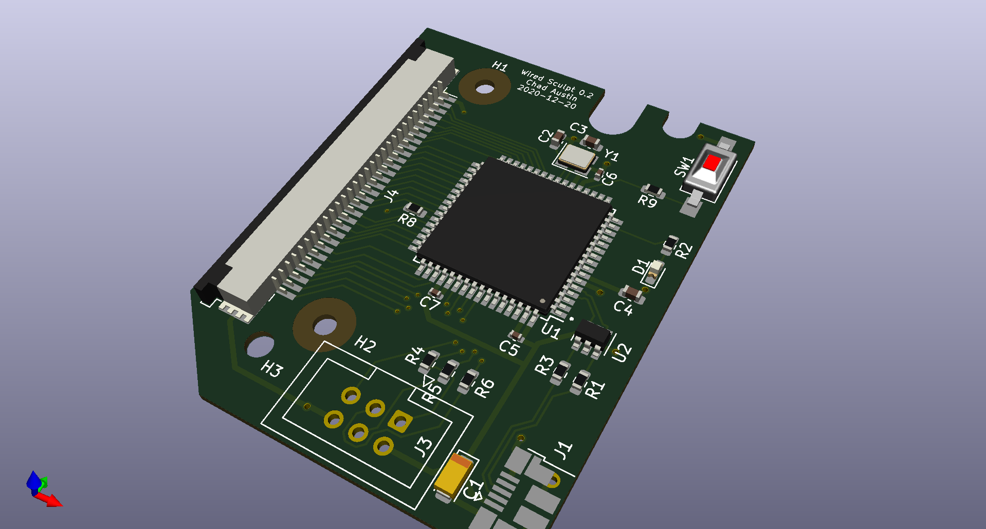
I found myself getting lost in the abstractness of holes and traces and footprints, so it was helpful to ground myself by occasionally loading the PCB in KiCad’s 3D viewer.
Designing the Final Board - Manufacturing and Testing Physical Fit
I tried to find a low-cost prototyping service in the USA, but it looks like China is still the best option if you want a PCB manufactured and assembled for an amount I’m willing to spend on a keyboard.
I saw PCBWay recommended somewhere, and it seemed like a fine choice. Their site has tutorials that walk you through submitting your Gerber files in a way they can process.
Before buying any components or doing assembly, I figured it would be smart to do a test order, just to physically look at the board and make sure it fit.
Good thing, because it didn’t! The mounting holes were about half a millimeter off, and the clearance was tight enough that half a millimeter mattered.
I couldn’t stop playing with it! It’s so magical to have the lines drawn in software turned into physical fiberglass and copper.
Designing the Final Board - Assembly
After making a couple adjustments and updating the version number and date on the silkscreen, I sent another order to PCBWay, this time requesting assembly service.
Overall, I was impressed with their communication. They couldn’t get the specific LED I’d listed in my BOM and confirmed if a substitution was okay.
Then, after all the parts were sourced, they asked me to clarify the polarity of the main tantalum bypass capacitor, since I’d forgotten to indicate anything on the silkscreen.
Finally, before shipping the assembled board, they sent me high-resolution photos of each side and asked me to confirm orientations and assembly.
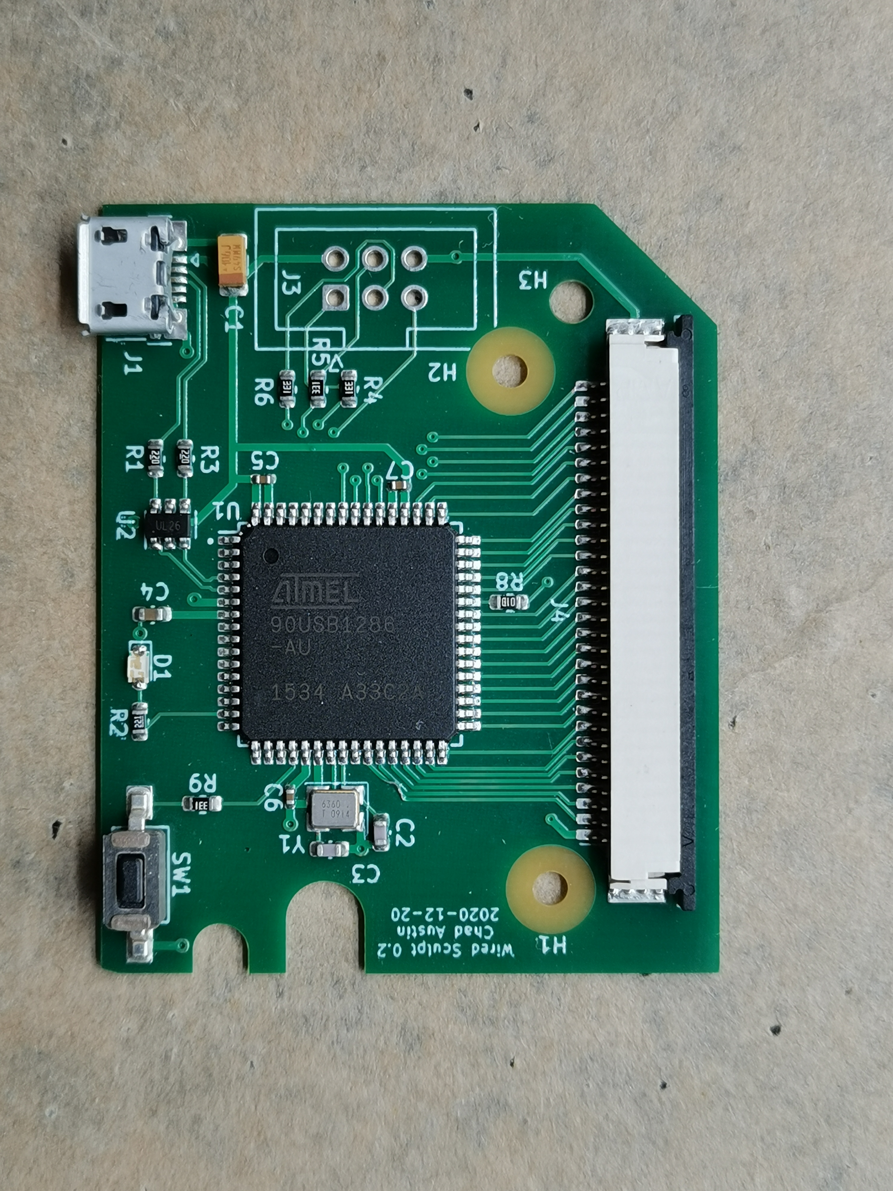
It all looked correct to me, though I later noticed that one of the traces is lifted. (There is still connectivity, and it’s not a huge deal, as that trace is only connected to an LED that I haven’t gotten to work anyway.)
It took about a month for the assembled board to arrive. I checked the assembly status every day. Maybe next time I’ll expedite. :)
Overall, I was pretty happy:
- My first test order, the minimum, was cheap and came with a cute battery-powered LED Christmas tree ornament.
- They made my board even though it was technically smaller than their minimum size.
- They took care of setting up the alignment holes for the pick-and-place machine, and sent me individual boards. I didn’t have to do any panelization.
- Shipping from China seemed unreasonably fast, but I suppose that’s how things work these days.
Electrical Testing
Before powering anything, I carefully did an electrical connectivity test of the main power circuits. Wanted to make sure the first power-on wasn’t going to result in a puff of blue smoke.
I briefly panicked, thinking everything was installed backwards, until I discovered my crappy little multimeter, in continuity mode, runs current from COM to positive. So I kept thinking there was a short somewhere on the board, and I’d have to disassemble to debug it! In reality, it was showing the ESD protection circuitry correctly shunting current from GND to VBUS.
When I realized this and reversed the leads, everything was correct. (And I bought a nicer multimeter which doesn’t have this problem.)
There was an electrical issue, however! Most of the pins on the ribbon cable connector weren’t soldered down to the board. I don’t know if this is a solder mask issue with the footprint in KiCad or if the board wasn’t flat enough for the paste on each pad to connect upwards to the leg.
I was afraid of forming bridges between the 1 mm pitch fins, so I coated the entire area in flux and very carefully swiped solder upwards from the pad. It took three passes before I was able to measure reliable connectivity between each ribbon pin and the corresponding microcontroller leg.
I see why people use microscopes for this stuff.
Fuses and Firmware
Now that everything seemed electrically correct, it was time to plug it in. Success! The factory-supplied DFU bootloader device showed up.
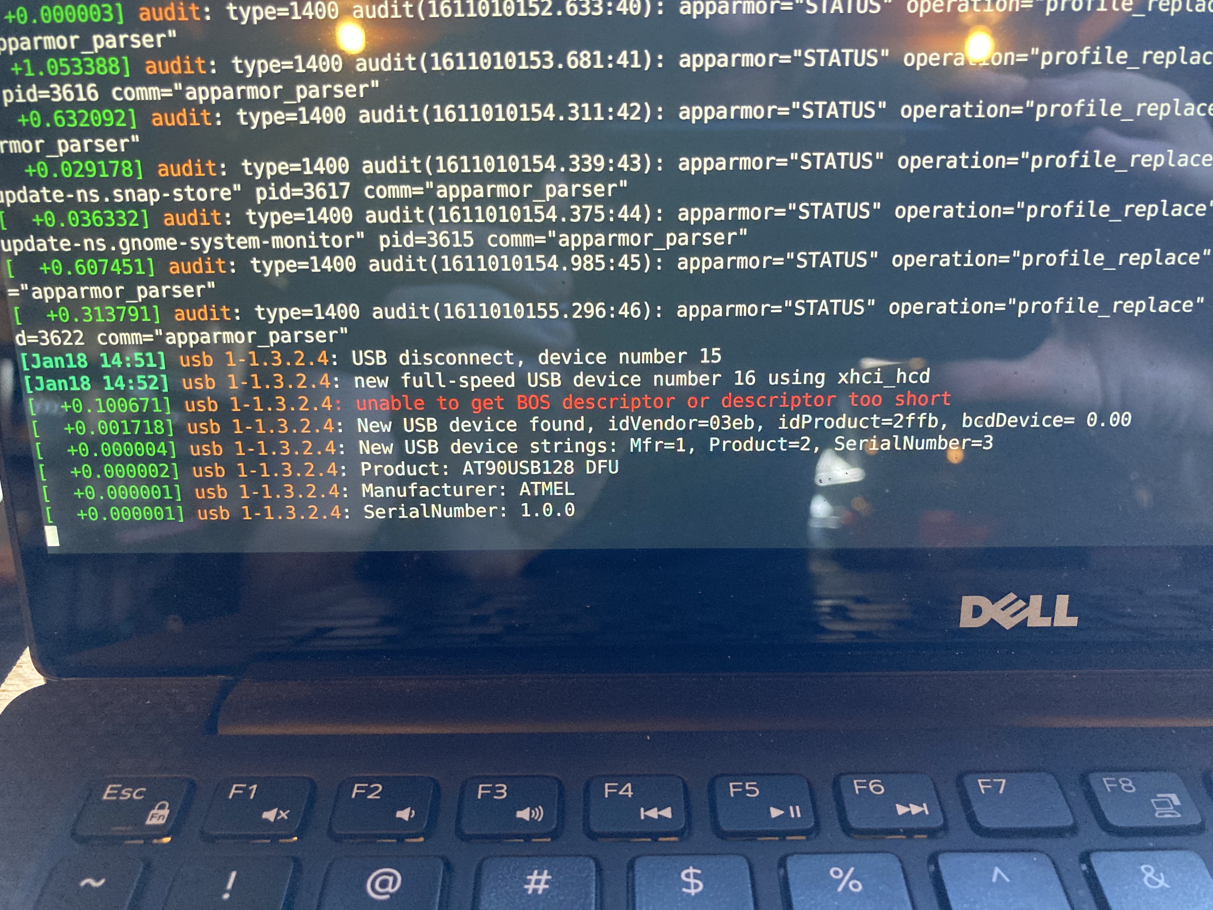
With dfu-programmer, I uploaded a tiny C program that simply blinked the test LED pin at 1 Hz. First weirdness: the clock speed seemed to be incorrect. After some careful datasheet reading, long story short, the CLKDIV fuse bit comes preprogrammed, which divides your clock speed by 8. So the crystal was 16 MHz, but the MCU was dividing that down to 2 MHz. I had expected it to use the internal RC oscillator by default, which would have resulted in a 1 MHz clock.
You can change the fuse bits with an in-circuit programmer device (not USB!), but that has the side effect of erasing the convenient factory-supplied USB bootloader, which I’d prefer to leave alone if possible. (There’s a LUFA bootloader you can upload, but since all of this was new, baby steps felt good.)
Fortunately, for this device, none of the above actually matters! It turns out I can get away without programming any fuse bits. CLKDIV merely sets the default clock speed divisor, and you can change it in software at the start of your program:
clock_prescale_set(clock_div_1);
The result of all of this is that the six AVR ISP pins on the board are only necessary in emergencies. (Good thing, because I borrowed two of the pins later.) From the factory, it can be flashed with firmware and function as designed.
QMK
After getting the clock speed issues sorted, I flashed QMK — thanks again to Michael Fincham for mapping the layout — and it worked!
The Sculpt treats left and right spacebar as independent keys. Michael took advantage of that and mapped right spacebar to enter. Turns out I couldn’t live with that, so I mapped it back to space.
Now that it’s not necessary for the battery indicator, I repurposed the keyboard’s red LED for Caps Lock.
I’d like to use the green LED too, but I discovered it has reversed polarity, and there’s no easy way to drive it with the current circuit.
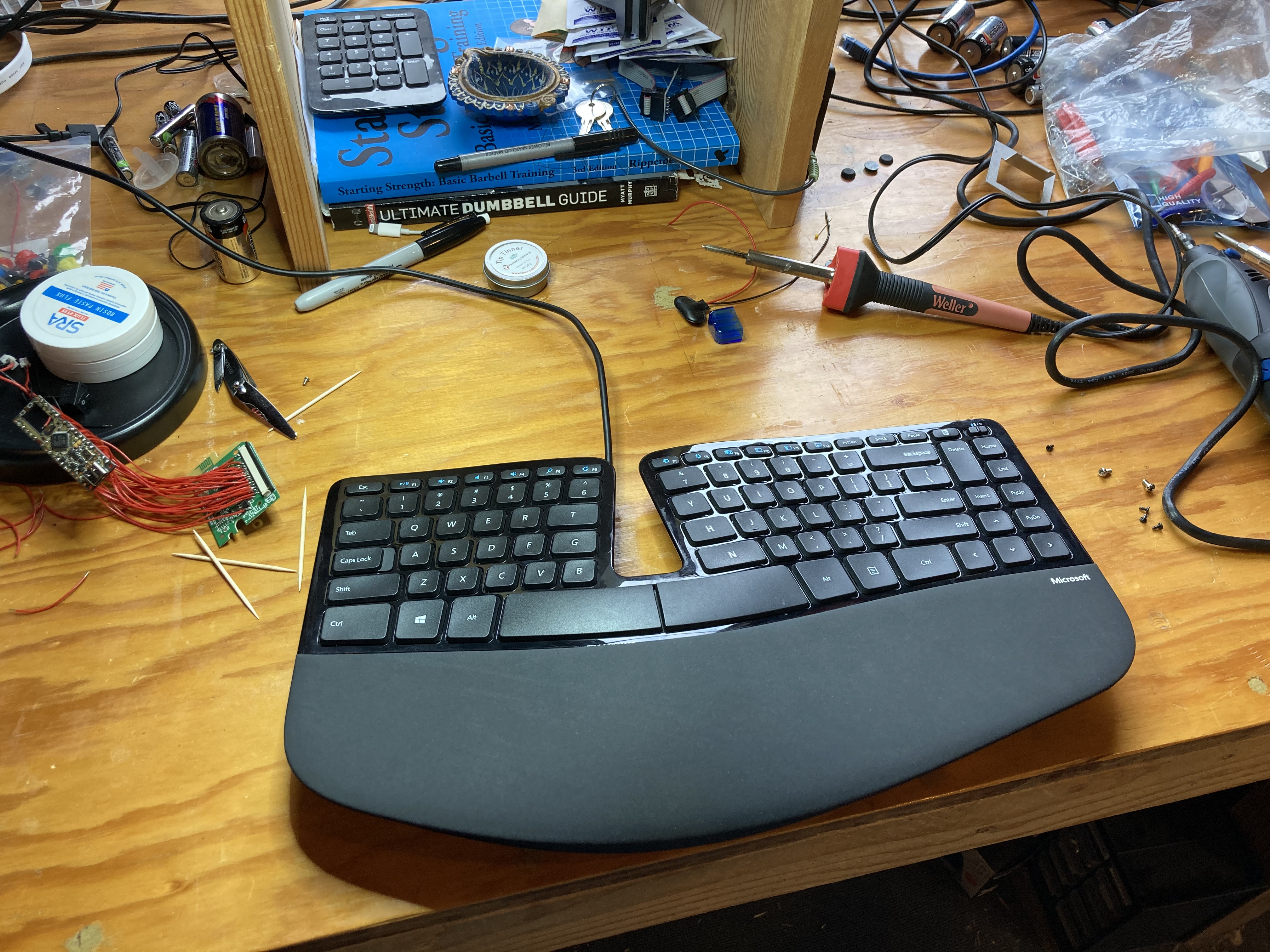
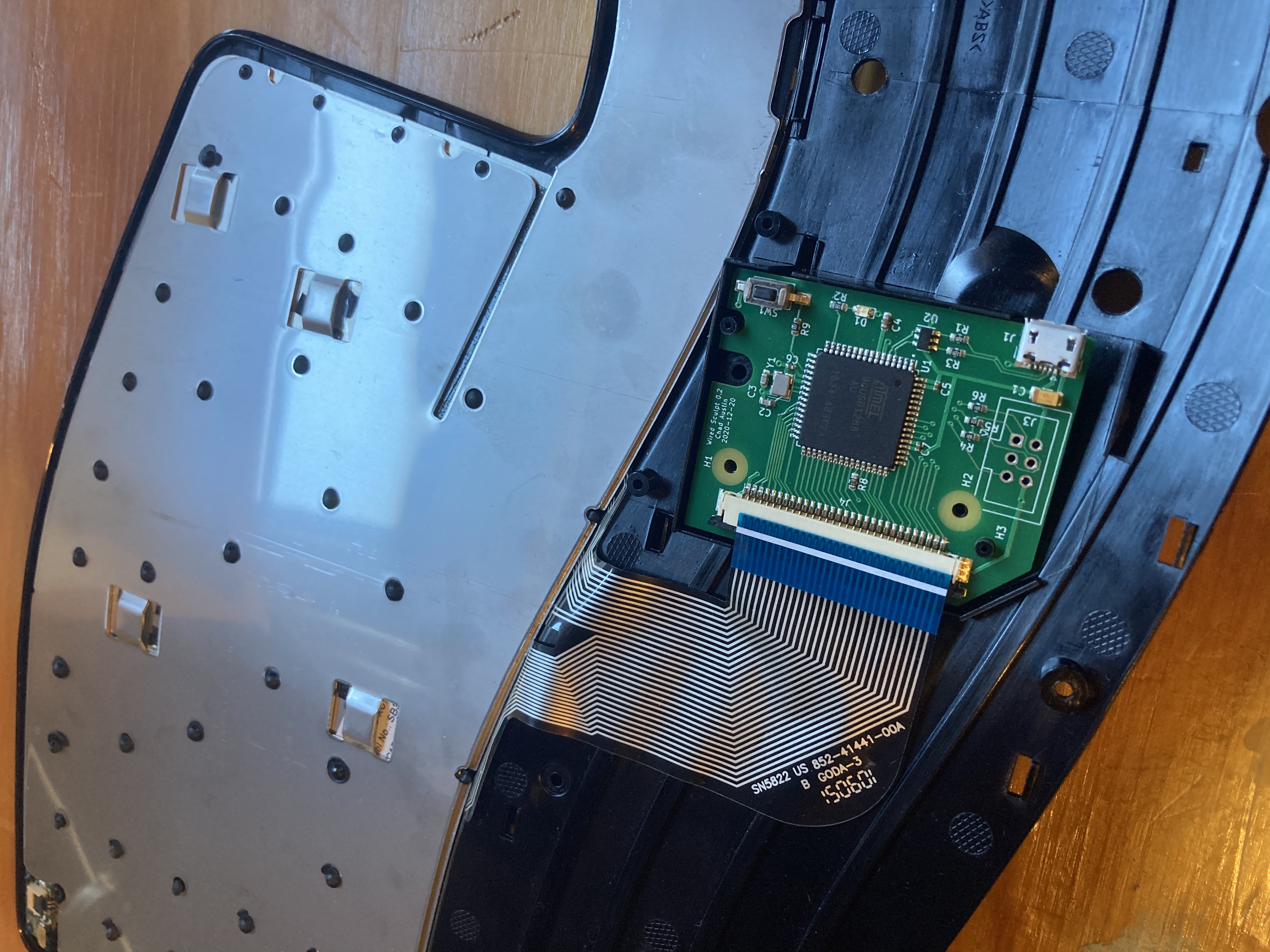
Case Fitting and Reassembly
Dremel.
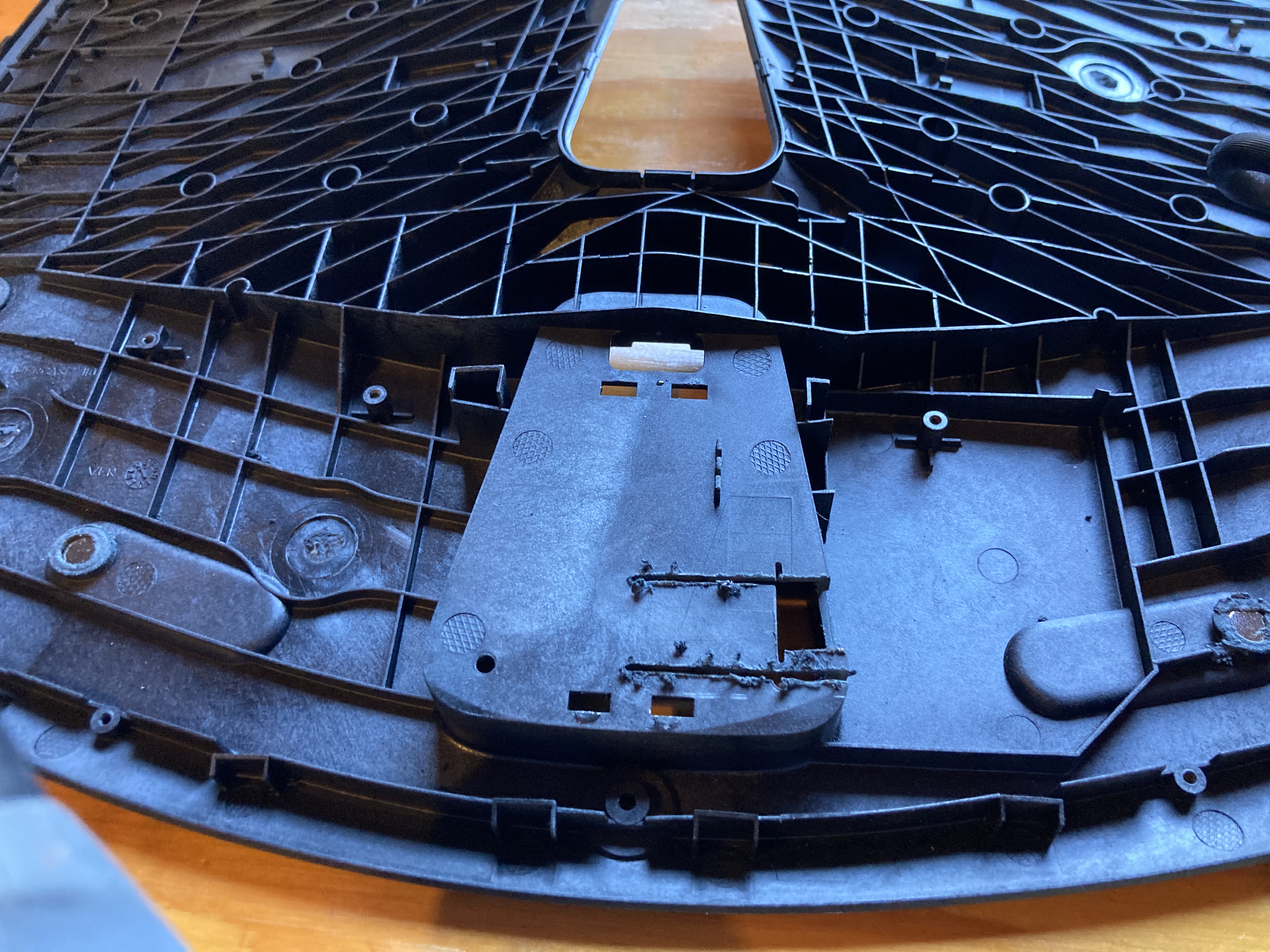
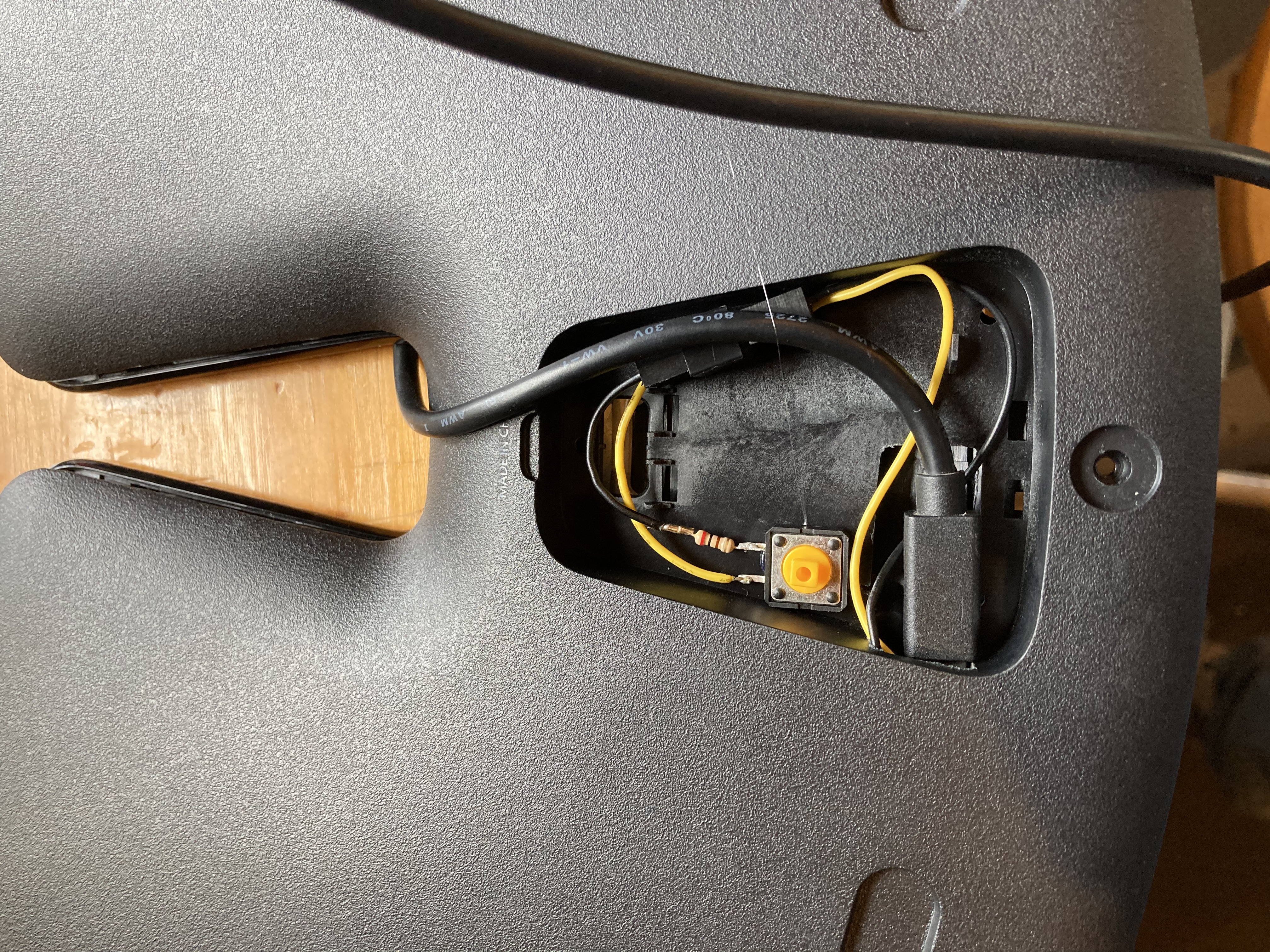
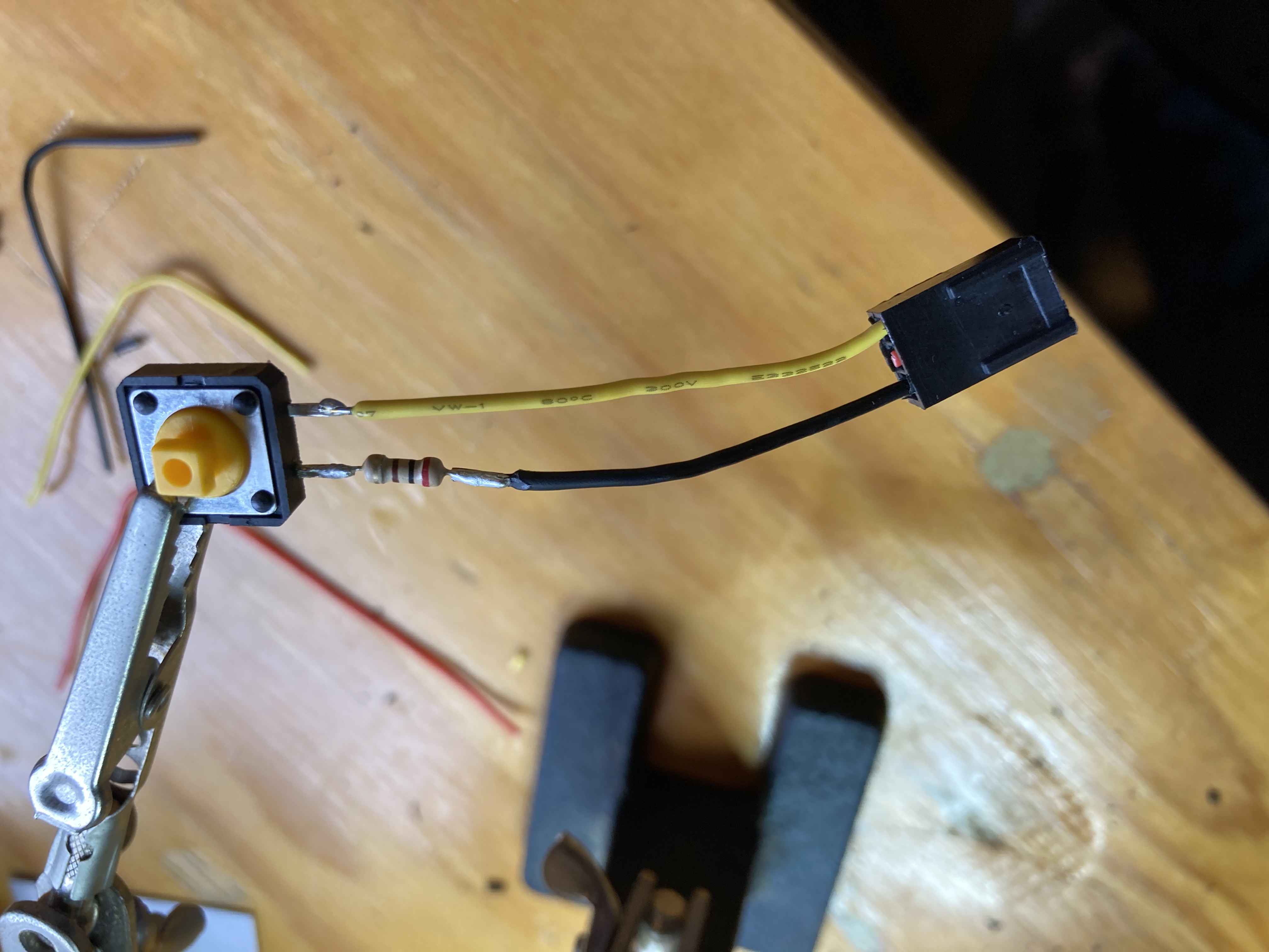
The only complication here was realizing it would be super convenient to launch the bootloader without disassembling the keyboard, so I soldered RST and GND from the AVR ISP pins to a button and hot-glued that into the battery compartment. (HWB is pulled low on the board, so all external resets enter the bootloader.)
To allow future disassembly, I cut up a PC fan extension cable and repurposed the connectors.
Latency
I don’t have enough words to convey how happy this modded keyboard makes me.
After years of thinking I was just getting old and losing my dexterity, my computer feels solid again. It’s like a bunch of resistance disappeared. Gaming is easier. Typing is easier. Latency is definitely better, and perhaps more importantly, more consistent.
I fired up Is It Snappy? and measured, on my PC, a total keyboard-to-screen latency reduction from 78 ms to 65. 13 milliseconds better!
I’ll have to test it on my new work laptop, an MSI GS65 Stealth, which measures keypress-to-pixels latency under 30 ms (!).
This project was worth every hour it took.
And during my latency testing, the wireless keyboard repeatedly dropped keys, as if to validate all of my complaints in a final hurrah.
Power
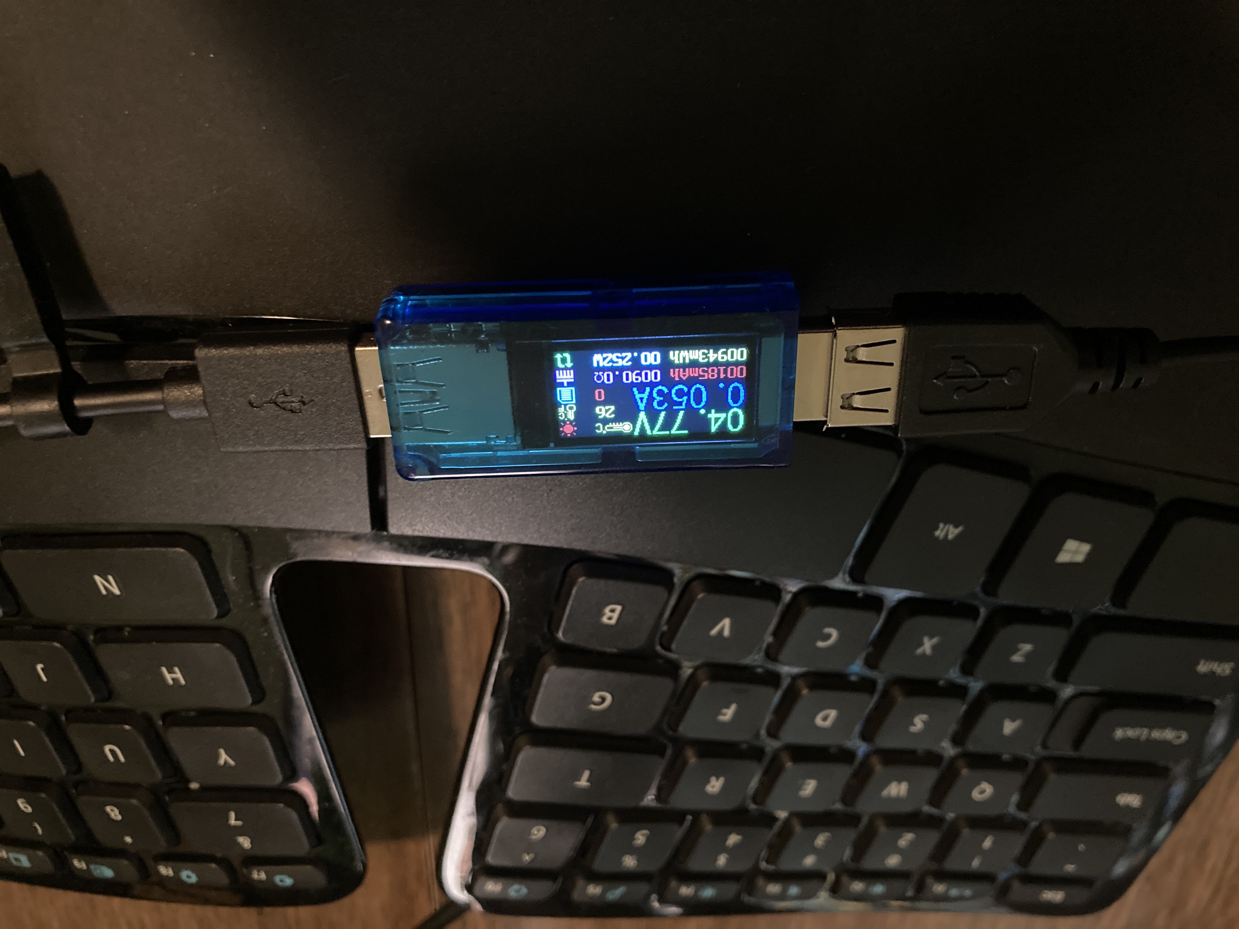
While waiting for the assembled PCB to arrive from China, I modded my Wii sensor bar to take 100 mA from the TV USB and bump it up to the 7.5V required to light its infrared LEDs. I was worried about excessive current draw and potentially damaging the TV’s USB ports, so I picked up a USB meter.
This keyboard draws about 60 mA — a quarter watt — which isn’t bad, but it feels possible to do better.
The original wireless transceiver draws 20 mA under use and under 100 µA when idle. So I might play around with clocking down to 8 MHz and seeing what subsystems on the microcontroller can be turned off.
With a switching regulator, I could even drop the MCU voltage to 3.3. And as awful as the wireless Sculpt’s sleep behavior was, there’s perhaps opportunity to improve there.
I probably won’t push too hard. I almost never use a wired keyboard on a phone or laptop where it might make a small difference.
Next Steps
Besides reducing power, there are a few improvements I’d like to make:
- The Fn switch (between function keys and volume/brightness/etc.) isn’t functional. I traced the membrane and discovered the switch controls whether pin 1 is pulled down by 47K or by half a megaohm. So I guess, assuming the membrane’s parasitic capacitance, I can detect the switch’s state by driving it high and measuring how long until it drops low.
- The green LED has reversed polarity from the red! To drive them both at once, I’ll have to set the ground pin at maybe half VCC and treat red active-high and green active-low. That might complicate the Fn switch, since it’s pulled towards this same “ground” voltage. I haven’t figured out what the Microsoft circuit does.
- Next time, I’ll put all LEDs on PWM pins. They’re a bit too bright, and breathing would be fun.
- I’d like a better-fitting ribbon cable connector. One that closes more nicely onto the ribbon. And while I appreciate being forced to learn the magic of flux, it would be nice if it came correctly soldered to the pads.
- Given tantalum is a rare earth metal, it might be nice to replace it with a ceramic and maybe a 4 Ω resistor in series. I’d love any input here.
- I’ve always kind of wanted a USB 2 hub like old keyboards used to have? Hub controllers are only a couple bucks…
- Pretty up the traces on the board. :) They should look as clean as Nilaus makes his Factorio belts.
Closing Thoughts
This was a ton of fun. Electronics is so hands-on and as someone who never held interest in Maker Faire or any of that community, I get it now. Connecting software to the real world feels so empowering.
What exploded my mind the most was how accessible hardware design is these days. Download the open source KiCad, pick some inexpensive parts on Digi-Key, send it off to a manufacturer, and for not that many dollars, you have a functioning board!
Now I stare at duct vents and wonder if I could just hook up a microcontroller and a servo to reduce home energy usage.
See discussion on Hacker News (2021).